
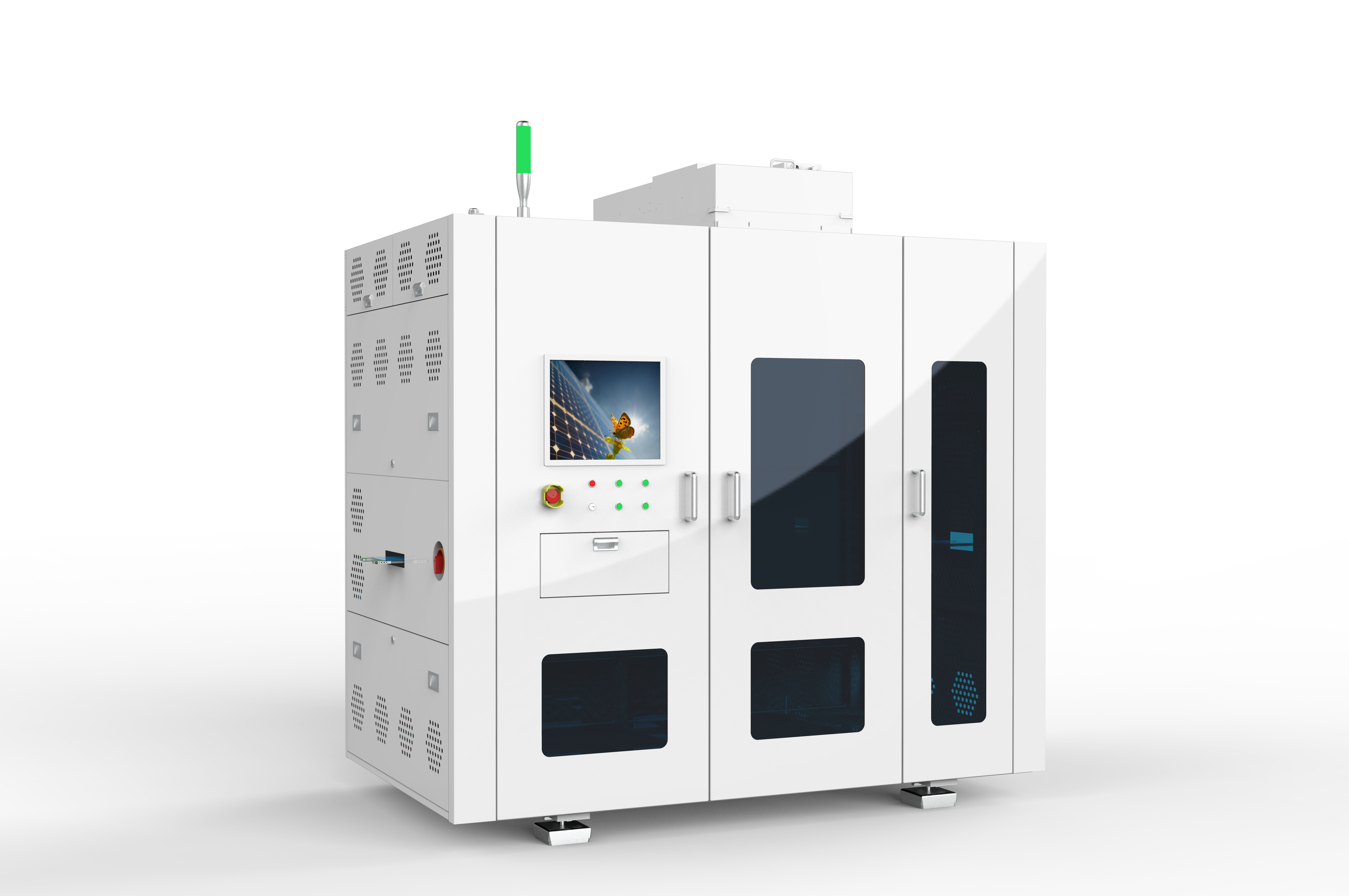
Product laser
Products

Enables ultra-narrow line widths with 20%–50% paste savings
Adjustable aspect ratio from 10% to 80%, minimizing shading loss and boosting light-to-electricity conversion efficiency
High print consistency enhances electrical conductivity; compatible with low-temperature pastes
Non-contact, pressure-free printing significantly reduces breakage rate
Compatible with customized line patterns to maximize light reflection in lamination and increase module output
Supports a wide variety of advanced solar cell architectures
Designed for high-volume manufacturing with scalable output
|
Specification |
Details |
|
Compatible Wafer Sizes |
Full, rectangular, or half-cut wafers (182 to 210 mm) |
|
Compatible Wafer Thickness |
100 to 180 μm |
|
System Throughput |
≥14,400 pcs/hour |
|
Grid Line Width |
10 to 15 μm |
|
Grid Line Height |
5 to 15 μm |
|
Aspect Ratio |
≥0.6 |
|
Production Mode |
Supports both offline and inline operation, compatible with printing line integration |

